Construction of all-optical logic gates using micro-optical resonators
Research
Construction of all-optical logic gates using micro-optical resonators
Theoretical analysis and presentation of issues for demonstration
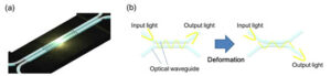
All-optical devices such as logic gates using micro optical resonators are expected to be realized due to their advantages such as low power consumption and signal multiplexing, but complex optical circuits have not yet been demonstrated. In this study, we propose an ideal all-optical logic gate configuration for actual system construction in which the input/output wavelengths match and the resonance wavelengths of all resonators are common, and numerically demonstrate its operation.
The basic element of the proposed residual light logic gate is an add-drop micro ring resonator shown in Fig. 1. The principle of the optical switch using this element is shown below. λ1 is out of phase with the resonator wavelength when there is no light input, but when the input is turned on, the resonant wavelength of the resonator matches λ1 due to the optical Kerr effect, and the input λ1 light is output to the drop side (Fig. 1(left)). When only λ2 is turned on, the light does not enter the resonator and passes through as it is because the separation from the resonant frequency is too large (Fig. 1 center). However, when both λ1 and λ2 are turned on, the resonance frequency first matches λ1, and as a result λ2 light also enters the resonator, the resonance frequency is further modulated to match λ2, and now the λ1 light is transmitted as is and the λ2 light is dropped.
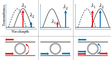
Fig. 1 Operation principle of a Kerr swich based on microring cavity
We analyzed a NAND gate composed of the basic elements shown in Fig. 1. All resonators are of the same design, and the only design parameters for constructing the logic gate are the way the resonators are combined and the coupling between the resonator waveguides. Fig. 2(a) shows the configuration and Fig. 2(b) shows the operation verification results. In this research, the effects of fabrication errors and input power fluctuation tolerance of the proposed circuit were also verified for the first time in the world for this type of optical logic circuit. This is the first time that such a circuit has been designed with a demonstration experiment in mind, and we will continue to search for a structure with even higher tolerance to fluctuations.
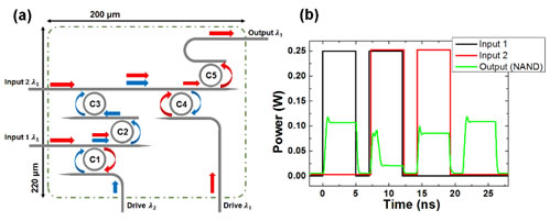
Fig. 2 (a) Photonic circuit design of a NAND gate.(b) Input and output waveforms calculated by CMT.
- Categories
- 研究トピックス