Ultra-compact, mass-producible photonic crystal wavelength divider Realization of ultra-compact, mass-producible wavelength divider
Research
Ultra-compact, mass-producible photonic crystal wavelength demultiplexers
Realization of ultra-compact, mass-producible wavelength demultiplexers
We can communicate with anyone, anywhere in the world. WDM (wavelength division multiplexing) communication technology supports this world of communication. We have succeeded in fabricating a wavelength division multiplexer for use in WDM communications in an ultra-compact and mass-producible manner.
WDM communication is a technology that increases the transmission volume by integrating many separate signals that need to be transmitted (or received) into a single transmission path (Figure 1(a)). Taking advantage of this feature, this technology has been often used for long-distance communications such as intercontinental communications, where a large amount of information must be transmitted at once. Looking around at the products we use in our daily lives, we can see that many of them are now equipped with communication functions. Until now, opportunities to transmit large amounts of information have been limited to long-distance communications, but considering the daily increase in the volume of communications, it is desirable to be able to transmit large amounts of information between servers, intranets, and even between chips in a single personal computer.
We have long been interested in silicon photonics, a research field in which silicon-based devices are used to realize optical communications. Silicon is the same material as the electronic elements used in personal computer chips, so we can say that silicon has a high affinity to be used in the same chip. Silicon also has the advantage of trapping light more tightly than other materials, making it possible to fabricate elements for optical communications that are smaller than those made from other materials. In silicon photonics, we have fabricated structures called photonic crystals. As shown in Figure 1(b), a photonic crystal consists of a thin silicon film with periodic holes in it. By making or not making holes in this periodic structure, various functions can be achieved.
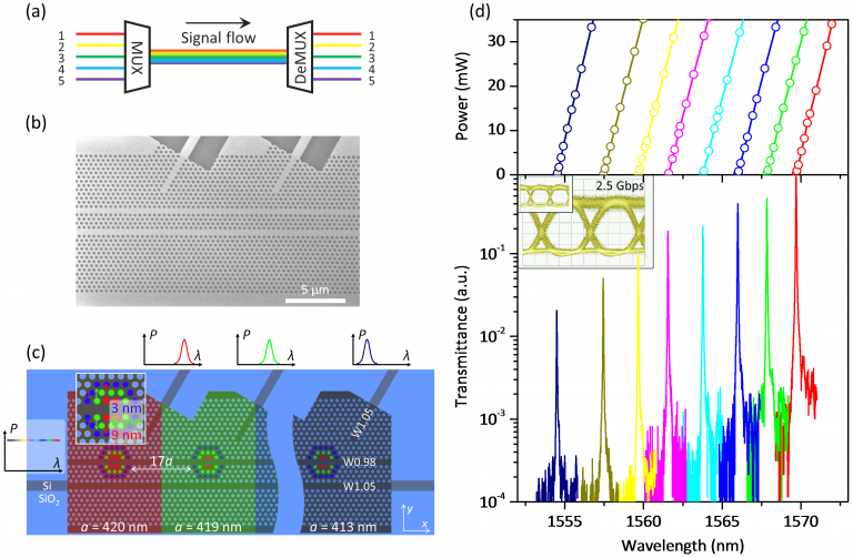
Fig. 1 (a) Schematic of WDM communication, where signals 1 to 5 are combined and transmitted by a wavelength multiplexer (MUX) and then divided by a wavelength demultiplexer (DeMUX). (b) Scanning electron micrograph of the fabricated wavelength demultiplexer. (c) Conceptual diagram showing the principle of operation of the wavelength demultiplexer. (d) Top: Result of adjusting the corresponding signal by applying heat. (d) Bottom: Transmission spectrum of the wavelength demultiplexer. (c) Center: eye pattern of a 2.5 Gbps signal. The inset shows the reference.
We have fabricated a wavelength demultiplexer for WDM communications using photonic crystals. A wavelength demultiplexer is a device that splits the integrated signal back to its original state in WDM communications. Figure 1(b) shows a scanning electron micrograph of the fabricated device, and Figure 1(c) illustrates the operating principle of the wavelength demultiplexer. Integrated signals are input from the left side of Figure 1(c) through a silicon (Si) thin-wire waveguide, and each signal is divided in the upper right direction. In this process, the signal passes through a structure called a width-changing resonator, which is shown in the enlarged figure at the upper left of Figure 1(c), and is then divided. By using a width-changing resonator, only certain signals can be passed through. We chose the width-changing resonator structure because our previous research has shown that it is compatible with our fabrication method, photolithography. The lower part of Figure 1(d) shows the transmission spectrum of the fabricated wavelength demultiplexer, which is able to demultiplex eight signals. The upper part of Figure 1(d) shows that the wavelength divider can be adjusted to accommodate various signals by applying heat. For example, applying 0~30 mW of heat to a green signal can be adjusted to accommodate signals from 1568~1570 nm. The center of Figure 1(d) shows the eye pattern of a red signal with a 2.5 Gbps signal input. Compared with the reference eye pattern shown in the upper left corner, the 2.5 Gbps signal can be transmitted without any problem at all.
Our wavelength demultiplexer using photonic crystals has the advantage of a device area that is 200,000 times smaller than that of conventional wavelength demultiplexers made from glass. In addition, the fabrication method we used, photolithography, has the advantage of mass production compared to electron beam lithography, which has been used to fabricate photonic crystal structures in the past.
- Categories
- 研究トピックス