Photolithographically fabricated silicon photonic crystal nanocavity photoreceiver with laterally integrated p-i-n diode
Research
Photolithographically fabricated silicon photonic crystal nanocavity photoreceiver with laterally integrated p-i-n diode
Towards a compact monitoring device for optical networks
With the development of technology, silicon photonic field has become one of its candidates. With the development of technology, silicon photonic field have become one of its candidates. In order to bridge the electrical circuits with photonic circuits, electro-optic and opto-electronic devices need to be developed. This is because at telecom wavelength, silicon is transparent and photo carriers could not be generated, Therefore, germanium integration on silicon commonly has been preferable. Still, this method is complex in fabrication and difficult to reduce CMOS compatibility. Still, this method is complex in fabrication and difficult to integrate with other CMOS devices. Furthermore, with the presence of defect, it increased the value of leak current.
Although recently low-power opto-electronic detection by all-silicon device in high Q PhC nanocavity has been reported, it has been demonstrated with an air-clad which requires a complex fabrication process. Therefore, in this study we demonstrated all-silicon photodetection using high Q PhC Two-photon absorption is used to detect light and we achieved low dark current (Thanks to the low dark current, the minimum detectable optical power is -20 dBm. By the demonstration of sub-GHz dynamic response, this shows that the photoreceiver can be used as a wavelength-selective photoreceiver. With the small noise detection, low detectable power and small footprint (50 μm2) make this device a good candidate as a cost-effective fiber monitoring system that is needed With the small noise detection, low detectable power and small footprint (50μm2) make this device a good candidate as a cost-effective fiber monitoring system that is needed.

Fig. 1 (a) Transmission spectrum and photocurrent at 10 μm input power as a function of the input wavelength. photocurrent (c) at various input powers when reverse -3 V is applied to the device
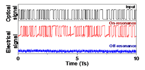
Fig. 2 0.1 Gb/s photoreceiver operation. the black waveform is the input optical signal, which is 255 pattern length of pseudorandom binary sequence. red and blue waveforms are the output electrical signal at the resonance and 0.1nm detuned, respectively.
- Categories
- 研究トピックス