Photonic crystal resonator using CMOS process
Research
Achieved the world's highest Q-value in CMOS process photonic crystal resonators
Toward the Integration of Photonic Crystal Technology and Silicon Photonics
Attempts are underway to reduce power consumption by processing information that is conventionally processed electrically in the form of light. In particular, research on silicon photonics, which aims to realize low-energy systems by replacing the wiring in chips with light, has been active. Current silicon photonics research focuses on the development of technologies related to the transmission of light within a chip, but in the future, signal processing may also be handled by light to achieve ultimate energy savings. For this purpose, elements called photonic crystal resonators, which can strongly confine light, are considered essential.
Based on this, the goal of this research was to incorporate photonic crystals as a new element in silicon photonics. The first is the difference in fabrication methods. Silicon photonics devices are now mostly fabricated by photolithography in the CMOS process, aiming at future integration with CMOS devices. The second difference is the structure. Silicon photonic devices are composed of SiO2(silicon dioxide), but conventional photonic crystals require a cross-linked structure. Therefore, it has been difficult to incorporate conventional devices on the same silicon chip.
It was thought that photonic crystals could not be fabricated with the precision of photolithography, the mainstream CMOS process, but this problem was overcome by adopting a design called the width variation type shown in Figure 1(a). In fact, in a resonator called L3, adjacent holes stick to each other, making it impossible to fabricate the device accurately.
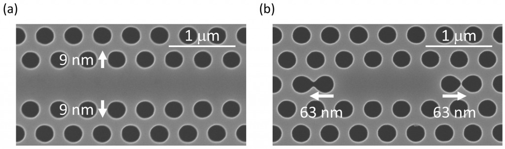
Figure 1: (a) Electron micrograph of the device fabricated in this study. (b) Conventional structure (L3 resonator) fabricated by photolithography.
Figure 2 shows the optical transmission characteristics of the device fabricated in this study. From the width of the transmission spectrum, a Q value of 2.2 × 10⁵The value is the world's highest for photonic crystal resonator devices fabricated by photolithography. This value is the world's highest for photonic crystal resonator devices fabricated by photolithography.qvalue of SiO2The device is covered from the top and bottom by an all-optical switch, which improves the life of the device. The all-optical switch operation of the device has also been realized, and it has been experimentally demonstrated that the device can be used for optical signal processing.

Figure 2(a) Transmission spectral characteristics of the resonator.
amount of moneyqvalue photonic crystals can be fabricated by photolithography, and similar to silicon photonic devices, SiO2The photonic crystal resonators could be fabricated on the silicon photonics substrate, indicating that photonic crystal resonators can be an elemental element of silicon photonics.
- Categories
- 研究トピックス
