EO modulator using randomness in photonic crystal line defect waveguides
Research
EO modulator using randomness in photonic crystal line defect waveguides
Control of fabrication errors and their practical use
Silicon photonics is a research field that uses silicon as a material to propagate light and handle optical signals. Compared to glass used for optical fibers, silicon has a higher refractive index, which allows light to be confined to a smaller space, making it possible to miniaturize devices and drive them with low energy. Photonic crystals are one of the elements belonging to silicon photonics, and have a special periodic structure that enables even stronger light confinement than silicon materials inherently provide. Various devices have been realized using photonic crystals, including waveguides, switches, detectors, and oscillators.
While photonic crystals enable miniaturization, they are susceptible to fabrication errors. Since the absolute amount of fabrication error is process-specific, the smaller the device to be fabricated, the greater the effect of the error. In addition, the recent trend in the fabrication process of photonic crystals is to use photolithography, which is capable of mass production but has lower fabrication accuracy, instead of the conventional EB lithography.
In this study, we have demonstrated that the effects of fabrication errors in photonic crystals can be structurally controlled and used with high yields. EO modulators are shown as a possible application, and operation at GHz has been confirmed.
We chose the structure shown in Fig. 1(a), which is called a photonic crystal line-defect waveguide. Light propagates through the center of the waveguide where there is no hole. Figure 1(b) and (c) show the cutoff frequency of this structure without and with fabrication error. When light is incident on the structure at the frequencies indicated by the red dashed lines and arrows, light confinement occurs only when there is a certain amount of fabrication error [Fig. 1(c)]. It is also important to emphasize that light confinement occurs only at W0.98 because the waveguide width is varied. Although this phenomenon originates from the randomness of the fabrication error, the structure allows us to control the area where the randomness appears.
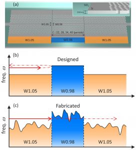
(a) Designed structure of PhC-WG, which consists of a W0.98 waveguide in between W1.05 waveguides. The inset shows the facet structure. (b) Band structure of designed (ideal) PhC-WG. The red arrow indicates the input light injected from the left side of the structure. (c) As (b) for the fabricated device containing disorder.
We also found that the probability of light confinement can be varied by changing the waveguide length of W0.98. 2D FDTD calculations show that the probability of light confinement can be varied by changing the waveguide length of W0.98 from 40a(ais the lattice constant), light confinement can be generated with high probability and transmittance can be kept high. The calculated results are in good agreement with the experimental results.
We have shown that light confinement due to fabrication errors can be used in a controlled environment in the form of EO modulation. The structure used is as shown in Fig. 2(a), where pn-doped regions are fabricated on both sides of W0.98 to allow current to flow. The experimental results are shown in Fig. 2(b) and (c), which were modulated at 500 MHz and 1 GHz. Although there have been devices using randomness in the past (e.g., laser oscillation using Anderson localization), from the viewpoint of practicality, it can be said that this research is the first practical development of a device using randomness.
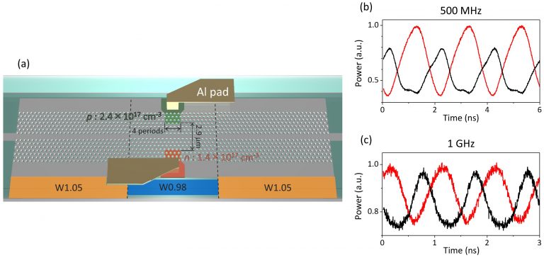
(a) Schematic illustration of the fabricated device. The device is clad with SiO2. (b) Detected output signals when a 500 MHz radio-frequency signal is applied. The red line is at the peak resonance, and the black line is when the input laser is slightly detuned at a wavelength shorter than the (c) As (b) but with 1-GHz modulation.
- Categories
- 研究トピックス