Development of an ultra-compact spectrometer using AI technology
Research Themes
Development of an ultra-compact spectrometer using AI technology
Contents
photonic crystalis an artificial crystal with respect to optical wavelengths. Just as semiconductor crystals have a band gap for electrons, microfabrication techniques can be used to create periodic structures of refractive index to create artificial materials with a band gap for light, called photonic crystals. The band gap can be used to strongly confine light within the chip or to slow the speed of light. The extremely small size of photonic crystals makes them a good candidate for the realization of optical integrated circuits.
However, photonic crystals and otherNanophotonics Devicesrequire extremely precise structures, and their performance has been limited by fabrication errors. Fabrication errors can cause fluctuations in the structure, resulting inLight localized randomlyThis phenomenon is called "Anderson localization of light. Although interesting as a physical phenomenon, such randomness is undesirable for engineering applications.
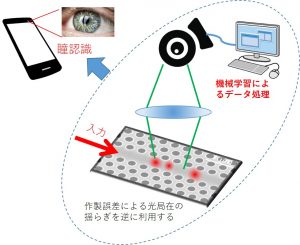
Image of the ultra-compact spectrometer configuration. Localization patterns are acquired and trained by AI.
But we have thisWe believe that randomness, on the contrary, can be used to improve the performance of the device by actively exploiting it.I'm trying to do it. To do so, we are trying to To do so, it is necessary toAI technology for data processingIncorporate the Software learning of localization patterns can improve performance if unknown responses can be predicted with a high degree of accuracy. One application is the development of a high-performance spectrometer. Conventional spectrometers are expensive and large, so they are used only for limited applications. If a compact and inexpensive spectrometer can be fabricated, it is expected to open up a variety of applications, such as integration into smartphones for pupil recognition or as a sensor in production lines.
Research Points
This research has just begun, and although proof-of-principle experiments have been conducted, can a truly usable device be realized? Will it work as desired for multiple wavelengths? There are still many unknowns, such as whether the device can really be used and whether it will work as desired at multiple wavelengths. Even if proof-of-principle experiments are completed, the next step is to find an implementation and a killer application that will be truly useful. This research is in its budding stage, and we are still groping in the dark, but it has great potential.
What makes research particularly difficult is that the neural networks used for data processing are black boxes, and it is not easy to understand how the computer thinks and derives its results. Neural networks themselves also require in-depth knowledge, requiring familiarity with both software and hardware.
In fact, the phenomenon in which light is localized due to the randomness of the structure is called random photonics, and is a field of great interest in the field of physics at the interface with statistics and chaos theory. HoweverEngineering Random PhotonicsThis research has the potential to set a precedent. This research is not only a simple spectrometer development, but also has academic value.
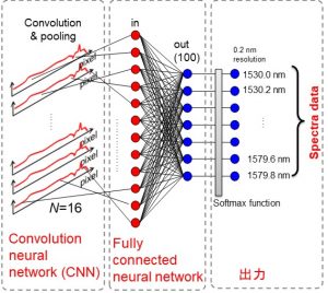
Neural network model used
Research Projects
This study has not yetbud stage (tooth)There is no full-scale joint research. However, a basic patent has been obtained, and future development of the project is highly anticipated. We are also working on machine learning with the advice of Professor Ikehara of the Department of Electronic Engineering.
《 Keyword 》
Photonic Crystals / Neural Networks / Machine Learning / AI / Random Photonics / Anderson Localization of Light
Tanabe Laboratory actively promotes collaborative research
Laboratory Information Session for FY2024 Assignees
We are holding a lab information session for students who will be assigned in 2024. Open Labs are free to come and go as they please. Individual information sessions are also available at any time.
Individual information sessions and lab tours are held in person. Please visit the Yagami Campus and see the experimental equipments in our laboratory. You can send us an e-mail or fill out the form below.