Silicon optical integrated circuits using photonic crystals
Research Themes
Silicon optical integrated circuits using photonic crystals
Contents
photonic crystalindicates word or phrase being definedArtificial crystals for optical wavelengthsJust as semiconductor crystals have a band gap for electrons, photonic crystals can have a band gap for light when fabricated using microfabrication techniques. Using the band gap for light, we can createLight can be strongly confined within the chip or the speed of light can be slowed down.The size is also extremely small. It is also extremely small in size.Optical Integrated CircuitIt is a strong candidate for one of the
Photonic crystals aresiliconThe technology is also expected to realize hybrid integrated circuits that combine light and electrons. This field, also known as silicon photonics, is expected to realize hybrid optical-electronic integrated circuits by integrating the strengths of light and electricity on a single chip, while separating the strengths of light and electricity.High-performance, low-power signal processing circuitsThe following is an example of a product that can be expected to achieve the following.
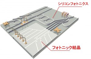
Photonic Crystal and Silicon Photonics Integrated Circuits
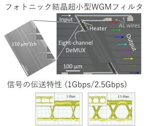
We have developed a series of high performance micro optical resonators made of silicon photonic crystals, all-optical switches, electro-optical modulators, photodetectors, and optical demultiplexers, which are the next key elements in optical circuits.
Key Technology Points
To visualize the behavior of light, electromagnetic field analysis techniques are required to solve Maxwell's equations using a technique called FDTD. This requiresComputed using massively parallel computersProgramming skills are also required. Once the program code is completed, it is not only a matter of changing the model, but also of making originality and ingenuity each time the subject changes.
high in performancePhotonic crystal micro optical resonatorsHow to fabricate photonic crystals and what combination of photonic circuits will work even in the presence of fabrication errors? Due to the high degree of freedom in the design of photonic crystals, there are many possible combinations, and only experience and deep consideration of lightwave engineering will reveal which of them should be selected.
Silica network formation by sol-gel method called TEOS
Silicon is an excellent material, but its performance is known to be inferior to that of III-V semiconductors in many aspects. There are a wide range of issues to consider, such as performance, cost, and technological challenges.
Research Projects
This research is being conducted in collaboration with the National Institute of Information and Communications Technology (NICT) and the National Institute of Advanced Industrial Science and Technology (AIST), both of which have advanced nanofabrication process technology. Students are actually operating the equipment and fabricating devices by themselves. We also use overseas silicon photonics foundries with researchers from other universities. In the past, we also collaborated with NTT Basic Research Laboratories, which is the old home of Prof. Tanabe.
Elements can also be fabricated in the clean room of the four-university consortium in Shin-Kawasaki. Thus, through various channels, we are conducting research by fabricating elements by ourselves and collaborating with external research institutions.
In addition, silicon-based optical integrated circuit technology is said to be compatible with quantum computers, so it has the potential to be used as a common platform for both classical and quantum research.
Laboratory Information Session for FY2024 Assignees
We are holding a lab information session for students who will be assigned in 2024. Open Labs are free to come and go as they please. Individual information sessions are also available at any time.
Individual information sessions and lab tours are held in person. Please visit the Yagami Campus and see the experimental equipments in our laboratory. You can send us an e-mail or fill out the form below.